Facilities
-
Combined Scanning Laser Doppler Vibrometer and White Light Interferometer

-
Base unit (GAN621C1) with a 900nm super luminescent laser diode providing over 150 nm of bandwidth
-
Capable of 3.0 μm axial resolution, an imaging depth of 1.9 mm in air and a line scan rate up to 248 kHz
-
Coupled with a scanning system (OCTG9), and a scan lens kit (OCT-LK2-BB) of 4.0 µm lateral resolution

-
Custom-made tribometer to study the friction forces at the interface of fingertip and various substrate
-
Utilizes a feedback control loop to keep the normal forces constant during the experiment while maintaining contact angle

-
Picosecond 515nm green laser cutter for advanced PCB research and development
-
Laser cutting, drilling and controlled depth engraving
-
Can be used to cut or ablate materials such as PCBs, Si wafers, glass, metals and polymers such as PDMS, PET, and Polyimide

-
COHERENT Chameleon Ultra femtosecond laser with COHERENT Optical Parametric Oscillator (OPO-VIS) wavelength extension
-
Two-tint (785nm) detection with modulated probe beam
-
Capable of high throughput through-plane and in-plane thermal transport analysis
-
Integrated with high precision thermal control stage (-190°C to 400°C) for measuring sample properties at different temperatures

-
Custom high voltage environmental capability for nanoscale electroadhesion and electrowetting studies

-
Biometric system capable of providing seamless insight into:
-
Eye tracking - Tobii Pro Glasses 2
-
EEG - ABM B-alert X24 EEG Headset
-
ECG and EMG - Biopac MP160
-
Facial expression measurement
-

-
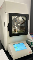
High vacuum thin film deposition instrument for FE-SEM imaging and TDTR measurements
-
Fully automated two-target process for metals such as Au, Ti, Al, Mo etc.

-
Automatic film applicator provides a reliable basis to apply coating films to flexible substrates in a uniform and reproducible way in order to eliminate variations caused by human factors
